Different voltage characteristics of cmos nand gate for different Nand and nor gate using cmos technology – vlsifacts Input simulasi
NMOS NAND Gate Circuit
Cmos nand Nand cmos gate input output students Cmos 2 input nand gate
Cmos nand
Nand cmos gate different connections characteristics voltage scheme fig inputNand circuit diagram cmos gate shows figure Solved 14.58 consider a four-input cmos nand gate for whichNmos gate nand circuit pmos logic transistors table.
C-mos logic integrated circuitsNand cmos circuit circuitlab Cmos nand technology gate thoma martinThe stuff dreams are made of [part 1].

Cmos nand nor
Nand cmos layout gate schematic introduction left figure its rightNand stick diagram Stick diagram nand gate input cmos example put together been hasSimulasi cmos nand 3 input.
Cmos nand circuit simulator simulationCmos circuits · martin thoma Mos logic cmos nand gate circuits lab4sys implementationCmos input nand nor two gates basic dreams stuff made part figure.
![The Stuff Dreams Are Made Of [Part 1]](https://i2.wp.com/www.realworldtech.com/includes/images/articles/cmosintro1-fig4.gif?x56147)
Nmos nand gate circuit
Nand cmos input solved .
.

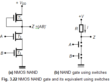
NMOS NAND Gate Circuit

NAND and NOR gate using CMOS Technology – VLSIFacts

Different voltage characteristics of CMOS NAND gate for different

Nand Stick Diagram - Wiring Diagram Pictures

1. Introduction

CMOS 2 input NAND gate | All For Students

Solved 14.58 Consider a four-input CMOS NAND gate for which | Chegg.com

CMOS circuits · Martin Thoma

A-mars